Perform the following tests:
Measure the voltages at the Emitter, Base and Collector of the transistor
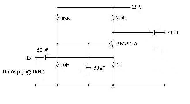
Here is the same transistor configured for Common Base operation
Perform the following tests:
1. Apply the input as shown
2. Compare the waveform at the OUT terminal with the input waveform .... are they identical ? What does this tell you ?
3. What is the p-p voltage at the OUT terminal ?
4. What is the no-load (NL) voltage gain of this transistor at 1kHz. ?
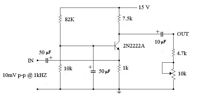
Here is the same circuit with a variable load
Perform the following tests:
1. Adjust the variable resistance for maximum voltage at OUT.... what is the value of this voltage ?
2. What is the resistance between OUT and GROUND when maximum voltage as above ?
3. What is the optimally loaded voltage gain of this transistor at 1 kHz. ?